WHERE TO BUY
Thank you for your interest in products and services from Socle Technology Corporation. We are pleased to offer you a wide range of trusted IC, electronic component products, total solutions and complete ASIC design service based in North America and the Asia Pacific. Please see our current contact information below and feel free to contact us if you have any questions about our products.
Buy Component
TAIWAN | CHINA | SEA | North America- TAIWAN -

Socle Technology Corp.(HQ)
300093新竹市科學工業園區研新三路3號5樓
5F., No.3, Yanxin 3rd Rd., Hsinchu Science Park 300093, Taiwan, R.O.C.
F: +886 3 563 3177
Socle Technology Corp. (Taipei)
114台北市內湖區機湖路32號9樓
9F., No.32, Ji-Hu Rd., Nei-Hu Dist., Taipei 11492, Taiwan, R.O.C.
- Authorized Distributors -

碩翊科技 SoiTech
13F., No.239, Sec. 1, Datong Rd., Xizhi Dist., New Taipei City 22161,Taiwan (R.O.C.)
P: 02-2648-0088#86113F: 02-2648-6978
Mail | Website- SEA -
- Authorized Distributors -

Sabre Technologies Pte Ltd
Tel : +65-62932003 Fax : +65-62930661
Mail:sales@sabre.com.sg | Website:www.sabre.com.sg
Supreme Components International (SCI)
Address : 62 Jalan Eunos, Singapore 419508 Phone : +65 6848 1178 Email:sharp@supremecomponents.com | Website : www.supremecomponents.com
- India -
- Authorized Distributors -

Unified GlobalTech (I) Pvt. Ltd.
Tel : +91-80-2229-0038 Tel : +91-80-43003868 Fax : +91-80-2229-0037
Mail:info@unified.co.in
Supreme Components International (SCI)
Address : #291-B, 3rd Main, 5th Cross, RR Layout, Bangalore – 560056, India Phone : +91-80-28482650 Email:sharp@supremecomponents.com | Website : www.supremecomponents.com
- Australia -

- CHINA -
虹晶电子(上海)有限公司
上海市浦东新区居里路123号4号楼402室
Solce Technology(Shanghai) Corporation / Room 402,Building 4,No 123 Juli Road, Pudong New District, Shanghai China
P: +86 21 6886 9895 P: +86 21 6886 9189
虹晶电子(上海)有限公司 -- 深圳辦事處
No.2, 2nd Donghuan Road,10th Yousong Industrial District, Longhua, Baoan, Shenzhen City, Guangdong Province,China 518109
P: +86 15162378393 +微信 15162378393- Distributors -


上海大毅经贸有限公司 Shanghai Dayi Trading Limited
深圳
上海市中山北路2911号中关村科技大厦1503-1504室
P: +86 021-6223-8600
- North America -
- Authorized Distributors -

Digi-Key Corporation
701 Brooks Avenue South, Thief River Falls, MN 56701, U.S.A.
P: +1 218 681 6674F: +1 218 681 3380
Website
Future Electronics, Inc.
237 Hymus Boulevard, Pointe-Claire, Québec H9R 5C7, Canada
P: +1 514 694 7710F: +1 514 695 3707
Website
Mouser Electronics, Inc.
1000 N. Main Street, Mansfield, Texas 76063, U.S.A.
P:+1 800 3466873Website
WPG Americas Inc.
5285 Hellyer Avenue, Suite 150,San Jose, CA 95138, U.S.A.
P: +1 408 392 8100F: +1 408 436 9551
Website
- Sales Representative -


O’Donnell Associates North, Inc.
2150 North First Street #433 San Jose, CA 95131, USA
P: 408-456-2950

Epic Canada
1925 18th Avenue NE, Suite 115 Calgary, T2E 7T8, Canada
P: +1 403 769 1881F: +1 403 769 1981
Epic Technical Sales, LLC (OR, WA)
Airport Executive Park 130-10691 Shellbridge Way Richmond, BC, V6X 2W8, Canada
P: +1 604 270 8758F: +1 604 270 3644
Epic Technical Sales, LLC (OR)
9400 SW Beaverton-Hillsdale Hwy Suite 140 Beaverton, OR 97005, U.S.A.
P: +1 503 292 7922F: +1 503 292 7903
Epic Technical Sales, LLC (WA)
11820 Northup Way Suite E200 Bellevue, WA 98005, U.S.A.
P: +1 425 822 9220F: +1 425 827 0350
EnVision LLC. (NC, TN, MS)
1400 Sunday Drive, Suite 101Raleigh, NC 27607, U.S.A.
P: +1 919 834 0505F: +1 919 834 3255
EnVision LLC. (GA)
1325 Satellite Blvd., NW, Suite 107 Suwanee, GA 30024, U.S.A.
P: +1 770 638 8998F: +1 770 638 2998
EnVision LLC. (AL)
4835 University Square, Suite 1Huntsville, AL 35816, U.S.A.
P: +1 256 721 1788F: +1 256 721 1789

Genesis Associates (MA, NH, ME, IR)
217 Middlesex Turnpike, Suite 205 Burlington, MA 01803, U.S.A.
P: +1 781 270 9540F: +1 781 229 8913
Genesis Associates (CT)
3000 Whitney Avenue, Box 202 Hamden, CT 06518, U.S.A.
P: +1 781 270 9540F: +1 203 314 8308

Oasis Sales Corporation (N. IL)
925 N. Plum Grove Road, Unit C Schaumburg, IL 60173, U.S.A.
P: +1 847 805 9500F: +1 847 805 9510
Oasis Sales Corporation (WI)
N27 W23953 Paul Rd., Suite 102 Pewaukee, WI 53072, U.S.A.
P: +1 262 523 9045F: +1 262 523 9085

Trilogy Marketing, Inc. (MI, KY)
One Towne Square Suite 260 Southfield, MI 48076, U.S.A.
P: +1 248 643 4344F: +1 248 643 4369
Trilogy Marketing, Inc. (OH)
30775 Bainbridge Rd., Ste., 220 Solon, OH 44139, U.S.A.
P: +1 855 838 9551F: +1 440 349 0381
Trilogy Marketing, Inc. (IN)
7255 N. Shadeland Ave., Suite A Indianapolis, IN 46250, U.S.A.
P: +1 317 863 4515F: +1 317 577 0852
Trilogy Marketing, Inc. (PA)
531 Corey Drive N. Huntingdon, PA 15642, U.S.A.
P: +1 724 861 4111F: +1 724 861 4112
- TAIWAN -
Socle Technology Corp.(HQ)
300093新竹市科學工業園區研新三路3號5樓
5F., No.3, Yanxin 3rd Rd., Hsinchu Science Park 300093, Taiwan, R.O.C.
F: +886 3 563 3177
Socle Technology Corp. (Taipei)
114台北市內湖區機湖路32號9樓
9F., No.32, Ji-Hu Rd., Nei-Hu Dist., Taipei 11492, Taiwan, R.O.C.
- CHINA -
虹晶电子(上海)有限公司
上海市浦东新区居里路123号4号楼402室
Solce Technology(Shanghai) Corporation / Room 402,Building 4,No 123 Juli Road, Pudong New District, Shanghai China
P: +86 21 6886 9895 P: +86 21 6886 9189
虹晶电子(上海)有限公司 -- 深圳辦事處
No.2, 2nd Donghuan Road,10th Yousong Industrial District, Longhua, Baoan, Shenzhen City, Guangdong Province,China 518109
P: +86 15162378393 +微信 15162378393
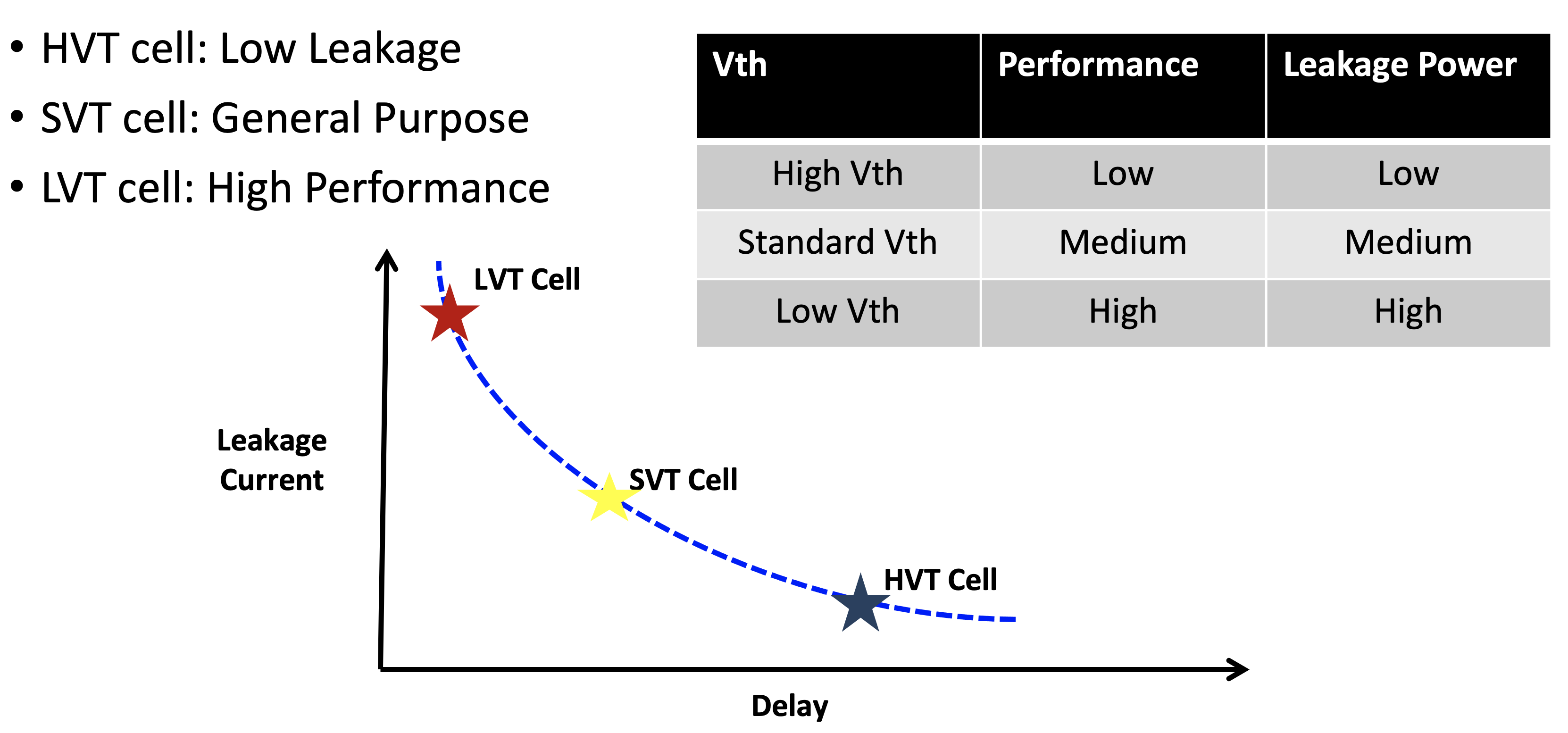
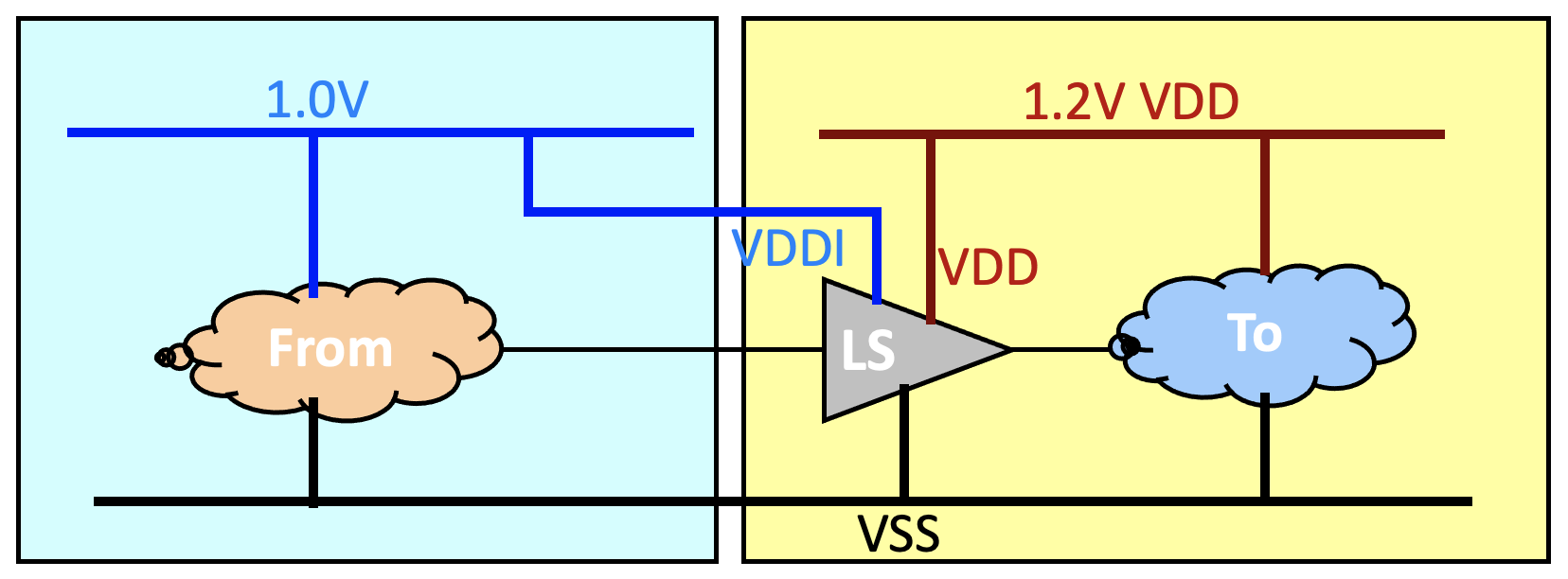
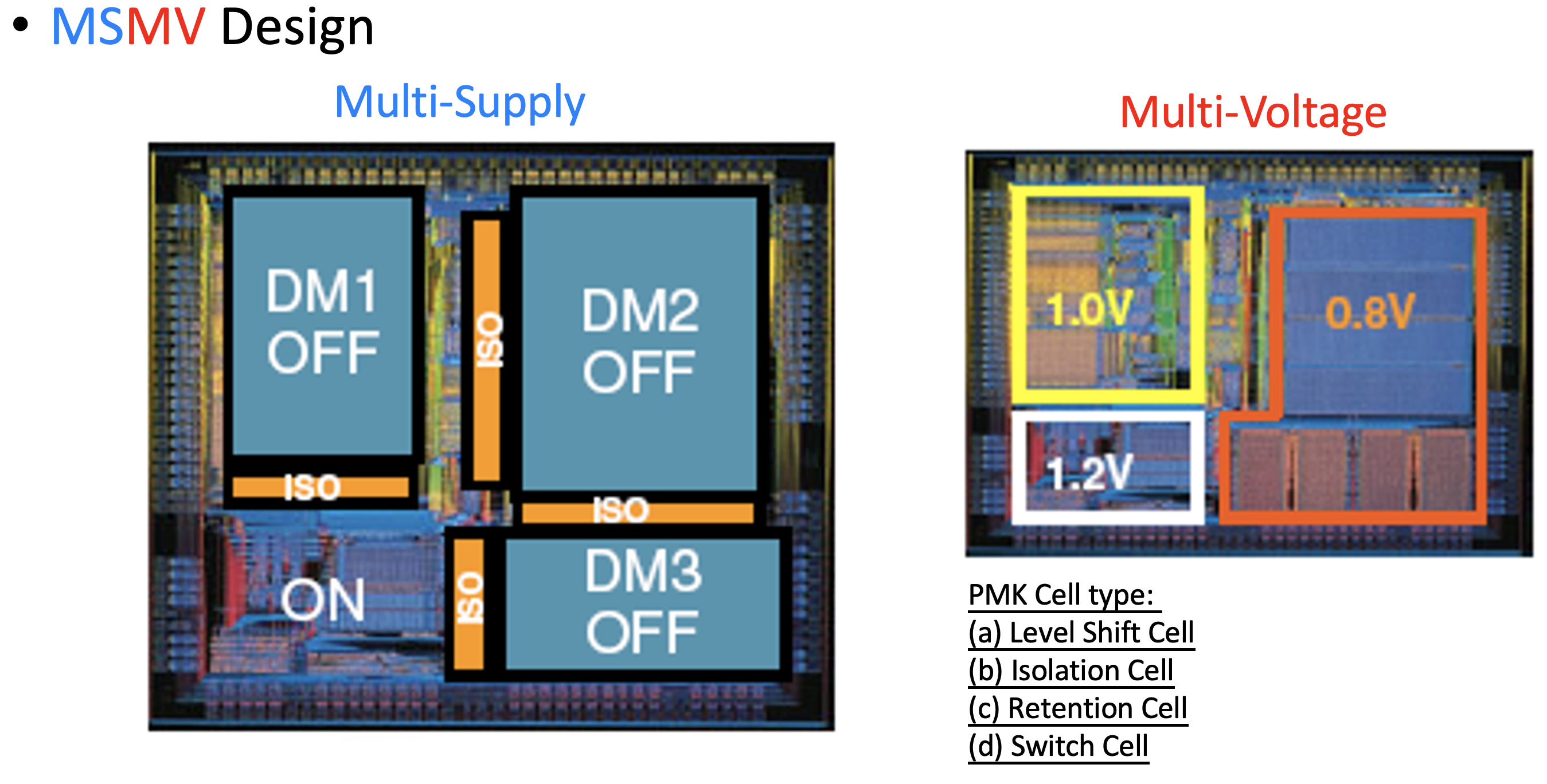 Level Shift Cell: A level shifter cell used by different voltage level(VDDI & VDD)